My Z80 System Design
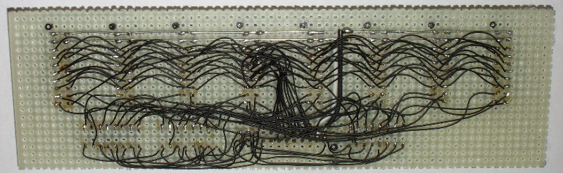
I'm creating this page to document my Z80 system design, mostly because I think it's cool, but also because there are so many Z80 system schematics on the internet that make me want to vomit. Someone needs to inject some sanity into Z80 system design, and apparently I'm the only one who is sane. So, let's get this over with...Since it's always best to start with a picture, here's a picture:
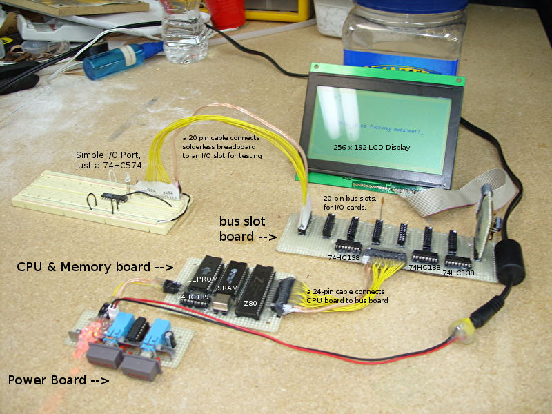
Now, to explain why that is so fucking awesome...
Multiple Board Computer
Somehow "single board computer" has come to be what people search for when they're looking for a cool little electronics project. However, you don't want a single board computer, and here's why:
Multiple boards means fewer components. This may seem like a paradox, but it's easy to explain: If you've committed to not having your I/O devices on expansion cards, then you must include every peripheral you might want on your single board. If instead you can expand your system later, then you can forget about all of the peripherals until you decide you need them.
Multiple boards also means reusable boards. You see that 8-slot bus board in that photo? If I decide I need a new peripheral, I just plug it in. If I need more slots, I can build a new 16-slot version and swap it out. If it were a single board computer, I'd have no choice but to rebuild the entire thing when I wanted to make modifications. I also have a version of the CPU board (built entirely on solderless breadboard) which allows my PC to program the EEPROM without removing it. When I want to test new code, I can simply connect the bus board to the CPU board I built on solderless breadboard, and when I'm done testing code, I can switch back to the much smaller non-reprogrammable board.
Also, multiple boards simply aren't a hassle in any way. I don't know why single board computers have become popular, other than for the same reason that calling something "viral" has come to sound like a compliment. If every cool little Z80 system you've ever seen has been a single board computer, then in your mind, "single board computer" is probably going to become synonymous with "cool little toy computer."
So don't be concerned that I haven't built a single board computer. Besides, if you really want to, you can put all of the components on a single board. I wouldn't recommend it, but it is certainly possible.
I/O Bus Slots
I/O Bus Features
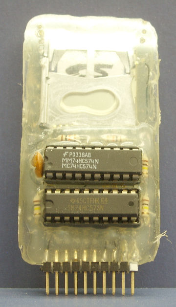
The most important property of a computer bus is that expansion cards are easy to make. You see that card that the LCD is attached to? The only thing on that card is a voltage generator for the -10 volts required by the LCD. Otherwise it just connects the LCD's I/O lines to the I/O bus as all of the address decoding is already handled by those three little chips on the bus board. You see that solderless breadboard on the left? It has a 74HC574 (a edge-triggered latch) serving as an output port, so that I can make that LED blink. (Blinking LEDs are the ultimate goal of all electronics projects, after all.) Again, no address decoding is necessary because it's all taken care of by those three chips on the bus board.Here is a very simple SD card interface:
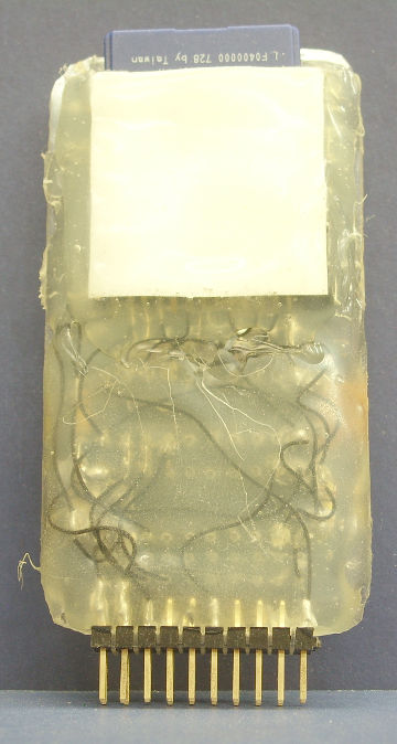
I went a little crazy with the hot glue, but as you can see, the only components are a 74HC573 used as an input port, a 74HC574 used as an output port, a few pull-up resistors for the SD card pins, and a capacitor for the supply voltage.
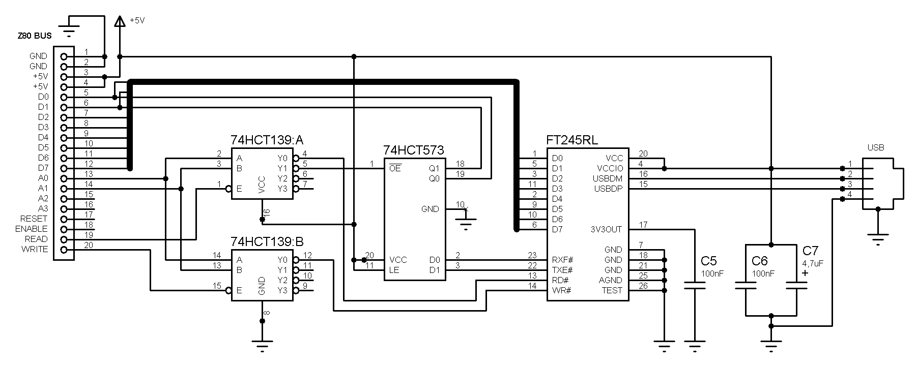
Here is a simple USB interface to allow the Z80 to talk to a PC:
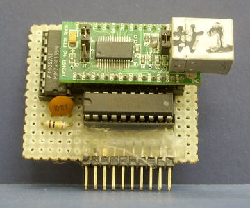
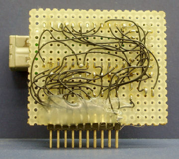
The chips on this board are an FT245RL for the USB communications, a 74HC573 used as an input port to check the FT245RL's status bits, and a 74HC139 used as an address decoder to select between the FT245RL and the 74HC573.
An anonymous reader sent me his scematic for essentially the same design, but based on a discrete FT245RL rather than the break-out board shown above, so this shows how the components above are used:
click for larger version
What enables these cards to be so simple is that much of the address decoding for I/O ports is done on the I/O bus board, where just three chips can decode addresses for eight bus slots. Most other bus designs simply pass all address lines to the bus cards and require them to fully decode their addresses, which requires several more chips on each expansion card, encourages poor address space management, and requires configuration jumpers on each card to prevent address conflicts. It's really much simpler if the I/O bus decodes addresses instead.
I/O Bus Pinout
I/O bus slot connectors are 20 pin connectors, with the following pinout:| Purpose | Pin | Pin | Purpose |
|---|---|---|---|
| Ground | 1 | 2 | Ground |
| +5 Volts | 3 | 4 | +5 Volts |
| D0 | 5 | 6 | D1 |
| D2 | 7 | 8 | D3 |
| D4 | 9 | 10 | D5 |
| D6 | 11 | 12 | D7 |
| A0 | 13 | 14 | A1 |
| A2 | 15 | 16 | A3 |
| RESET | 17 | 18 | ENABLE |
| READ | 19 | 20 | WRITE |
The order of these signals is largely intended to be easy to remember, but I also took into consideration the difficulty of routing traces on a circuit board, which is the reason for the odd order of the last four pins. RESET is the same signal on all slots, just like D0-D7 and A0-A3, so I grouped it with them, whereas ENABLE, READ and WRITE are unique signals for each slot, so I put them at the inside edge of the connector where routing those pins will be easier.
Pins 1 through 4 supply (or receive) power. Each power rail receives two pins not so much for concern of current requirements, but rather, to make it easier to run large traces or large wires to these pins by soldering directly across both of them. (See photos of bus boards.) Each card slot should be well-connected to the system's power bus such that one of the cards may be a "power card" that supplies power to the system. (Some elaborate power supplies may benefit from having I/O ports so that the CPU can monitor or control power.)
Pins 5 through 16 don't need much explanation. They should directly connect to the similarly-named Z80 CPU pins.
Pin 17, RESET, should be attached to a pull-up resistor somewhere in the system (either on the CPU board, the bus board, or the power board), such that any I/O card can trigger a system reset simply by pulling this signal low. (E.g., that "power card" may want to implement power-on reset, or have a reset button.)
Pin 18, ENABLE, is the logical OR of the Z80's IORQ pin, and the output of address decoding circuitry for the Z80's pins A4 through A7. It can generally be ignored, relying upon only READ and WRITE to trigger data transfers, but chips which accept a CS or CE input often consume less power when it is inactive and so you should connect it to such chips.
Pin 19, READ, is the logical OR of the Z80's IORQ pin, the Z80's RD pin, and the output of address decoding circuitry for the Z80's pins A4 through A7.
Pin 20, WRITE, is the logical OR of the Z80's IORQ pin, the Z80's WR pin, and the output of address decoding circuitry for the Z80's pins A4 through A7.
The signals on pins 18, 19 and 20 are unique to each card slot. Each slot is assigned 16 I/O ports from the 256 I/O port address range of the Z80. The upper four bits of the address are determined by which slot the card is inserted into, making address conflicts impossible and address configuration as simple as putting the card in the correct slot. Thus, each slot needs to decode only the lowest 4 address bits, and only to the extent that it cares to differentiate between them.
The ENABLE, READ and WRITE signals become active only when that particular card slot is being accessed. If ENABLE is active, there is an I/O request being made to one of that slot's 16 I/O ports. If READ is active, one of that slot's 16 ports is being read. If WRITE is active, one of that slot's 16 ports is being written to. All three signals are inactive when other I/O slots are being accessed or when system memory is being accessed.
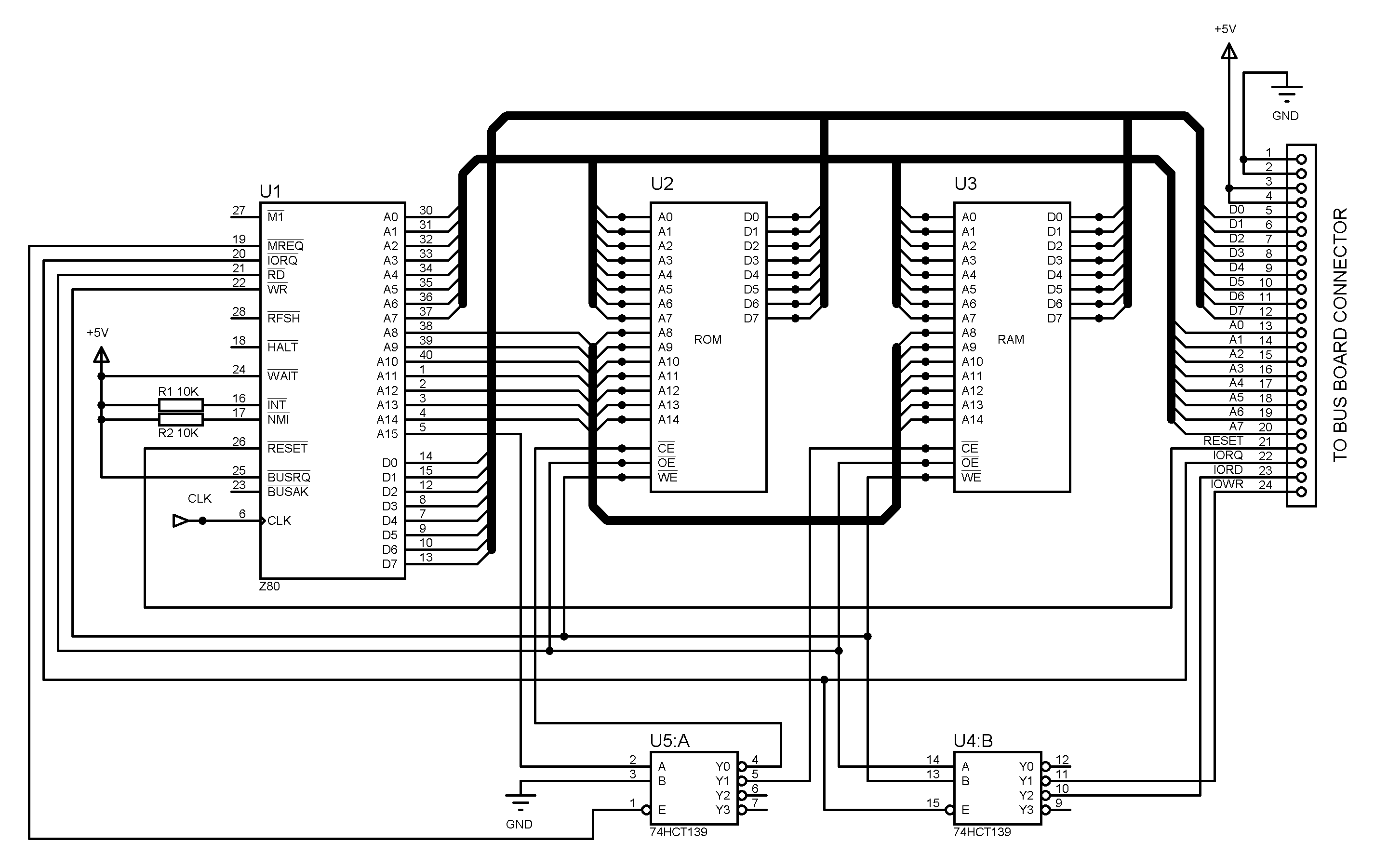
CPU & Memory Board
Minor Information
The CPU and RAM share a lot of signals (A8 through A15 and MEMRQ) that affect nothing else. This makes separating them from the I/O bus board a semi-logical idea. I suppose you could combine them if you like and still keep the same bus configuration, but I think that having them on a separate board allows for more flexibility, e.g. if you decide one day that you really need DMA and so you want to build a new CPU board with a DMA controller of some sort, you don't have to wire up a whole new set of bus connectors. Same goes if you decide you need a different memory layout.Schematic
Here's a schematic for the simplest Z80 system possible: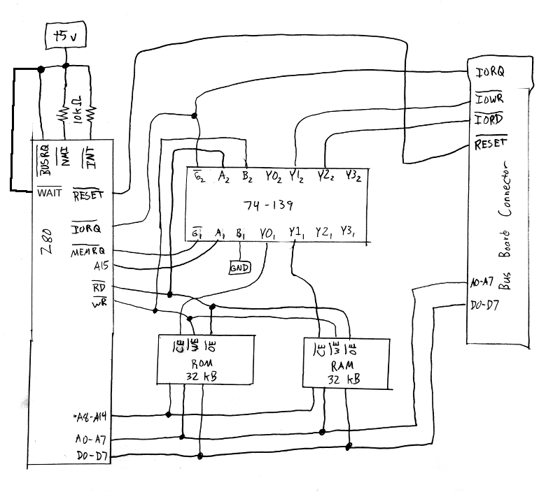
An anonymous visitor to this site contributed the following version of the above schematic, which some readers may prefer due to it's more traditional appearance. Be sure to click on it it get a larger version suitable for printing.
click for larger version
Not shown are power connections, the Z80's clock source and a bunch of unused Z80 pins that you can just leave unconnected. Also, tossing a 100 nF ceramic capacitor across the power rails somewhere is probably a good idea. Modern CMOS chips almost don't need these things anymore, but I have had issues which were solved by adding one. Indeed, that's why there's one stuck in one of the bus slots in the photo at the top of this page, as it didn't work until I added it.
Circuit Details
Memory Layout
I've never needed more than about 4 kB of EEPROM and 4 kB of SRAM, thus I've settled on using the simplest possible memory configuration of 32 kB of EEPROM in the lower addresses and 32 kB of SRAM in the upper addresses. While a full 32 kB of EEPROM is a bit much to boot an SD card, I figure I can use up the extra space by providing BIOS routines to access whatever hardware is in the system, allowing the programs on the SD card to be transferred between multiple such Z80 systems and still know how to access the SD card and LCD displays even if the hardware changes. ...and both have, as I have different types of LCD displays, and I've made two different SD card interfaces, the other one being much more complex but also much faster due to doing the SPI transfers in hardware rather than software.Port Addresses
While it is possible to abuse the fact that the Z80's "B" register is often the upper 8 bits on the address bus during port I/O requests to allow there to be 65536 ports, I've chosen not to do this simply because 16 ports per I/O card, and 256 ports total, is more than enough. Devices which use a lot of ports typically only use 8, and if something really needs more than 16 ports, it isn't that difficult to wire up a latch on that I/O card such that you can store address bits by writing to one port, then access the port at that stored address via another port. Thus, wiring up eight additional port address lines would seem to be nothing but a significant waste of effort.Interrupts
I have used interrupts on occasion, but never more than one at a time. Thus the interrupt pins are simply pulled high, and I tossed a small two pin header connector right next to the two interrupt pins on the Z80, figuring that location to be ideal as an identifier of what the pins are for, and also because it allowed me to toss the pins in as an afterthought.The interrupt pins allow whichever card needs the interrupt to be connected to the CPU board via a small one pin cable. Also, I can build an interrupt card which accepts multiple interrupt sources and provides some I/O ports for the CPU to manage interrupts as well as discover which interrupt routine needs to be called. In my opinion the Z80 interrupt modes which call the relevant interrupt handlers directly are unnecessarily complex. I don't care if my interrupts take ten extra clock cycles to execute, all I care about is that my CPU doesn't have to constantly check an I/O device just to verify that it still has no new data. Thus, checking an I/O card to discover the number of the interrupt that triggered doesn't seem like a huge deal to me, especially since it keeps me from including a complex circuit on the CPU & Memory board that I don't even need for 95% of potential applications.
Besides, only stupid old PC hardware like serial ports and parallel ports strictly requires interrupts anyway, due to a lack of hardware flow control. What is referred to as "hardware flow control" on serial ports is actually software flow control, simply performed with the RTS & CTS pins rather than via bytes in the data stream. Real hardware flow control has the hardware on one end informing the hardware on the other end when its buffers are full automatically.
With ordinary serial ports (such as the 16550A UART), if the Z80 doesn't respond immediately to the "buffer almost full" interrupt and respond by disabling the RTS signal, the PC will continue to send data and the UART's buffer will overflow. On the other hand, if you use an FT245RL to communicate with a PC over USB, then even if the Z80 gets lazy and fails to check on the FT245RL for an hour, it won't lose any data because when its buffers are full it tells the PC automatically and the PC stops sending data. Thus, if you just don't use stupid hardware, your need for interrupts largely vanishes.
DMA
I didn't include a DMA chip for the very good reason that there's more than one way to do DMA and so there's simply no way to plan for DMA that you don't presently need. For example, sound cards in PCs require a DMA controller which places memory addresses on the address bus on behalf of the sound card so that the sound card can simply activate a "DMA read" signal and grab a byte off of the data bus with no concern for where it came from. However, video cards generate their own addresses and so they need no such DMA controller and indeed it would only be in the way.Given that both FIFO buffer chips (look at the 74HC7030 for example) and dual-port memory chips (no recommendations) are available, both of which would allow you to do most things you'd do via DMA via simple I/O ports instead, DMA mostly seems like an unnecessary complexity. That said, it certainly does have its uses, but those uses are going to be best applied by a completely custom CPU & Memory board rather than any generic DMA circuitry. Thus, there's really no point in even thinking about it.
CPU & Memory Board Pinout
Here is the pinout for the connection between the CPU & Memory Board and the I/O Bus Board:| Purpose | Pin | Pin | Purpose |
|---|---|---|---|
| Ground | 1 | 2 | Ground |
| +5 Volts | 3 | 4 | +5 Volts |
| D0 | 5 | 6 | D1 |
| D2 | 7 | 8 | D3 |
| D4 | 9 | 10 | D5 |
| D6 | 11 | 12 | D7 |
| A0 | 13 | 14 | A1 |
| A2 | 15 | 16 | A3 |
| A4 | 17 | 18 | A5 |
| A6 | 19 | 20 | A7 |
| RESET | 21 | 22 | IORQ |
| IORD | 23 | 24 | IOWR |
This is largely self-explainatory. IORQ simply connects to the Z80 pin of the same name, while IORD and IOWR are the logical OR of IORQ with the Z80 pins RD and WR.
I/O Bus Board
Schematic
I can't draw a schematic for the I/O bus board. There are only so many little lines one can look at before going insane. However, it's just three 74HC138 which are easily explained. Even more easily explained in a picture that looks deceptively like a schematic: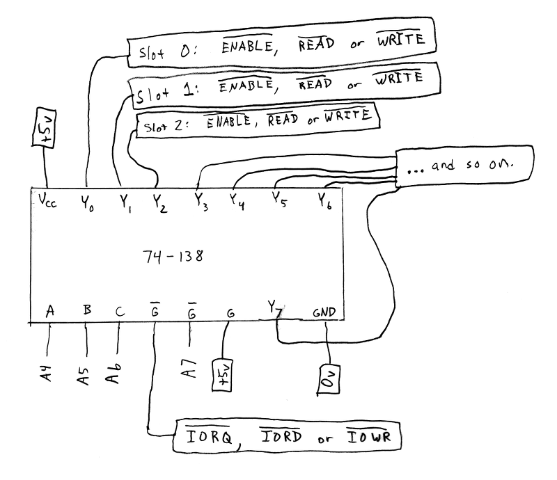
The same anonymous visitor mentioned above, apparently less prone to insanity caused by looking at little lines, also contributed a schematic for the bus board. Again, be sure to click on it it get a larger version suitable for printing.
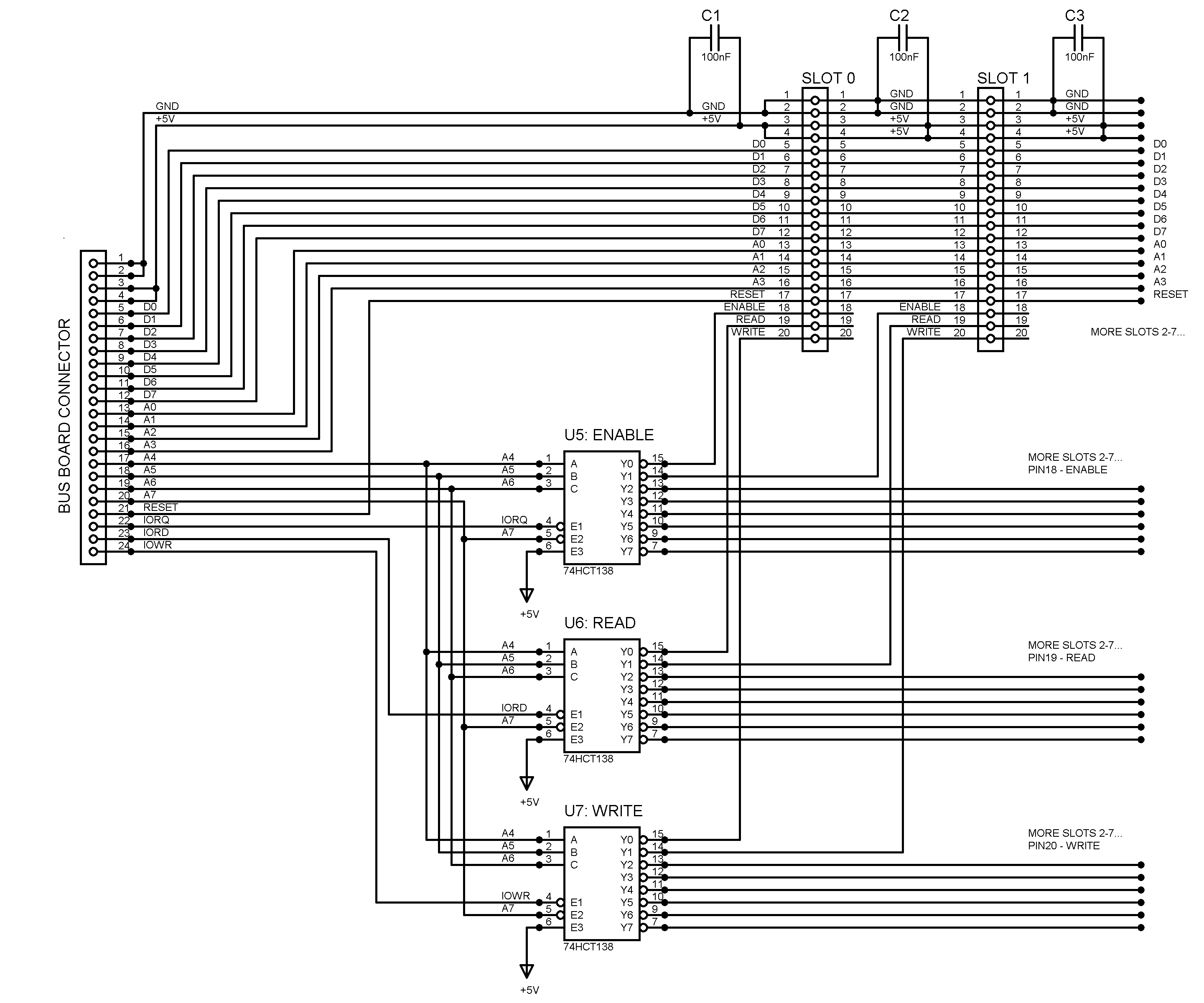
click for larger version
One each of the three 74HC138 is assigned to generate READ, WRITE or ENABLE signals. The one with IORD as an input generates the READ signals for each slot, the one with IOWR as an input generates the WRITE signals for each slot, and the one with IORQ as an input generates the ENABLE signals for each slot.
Additionally, if you want 16 slots instead of 8, you can generate the additional 8 sets of signals with three more 74HC138 in nearly the same configuration:
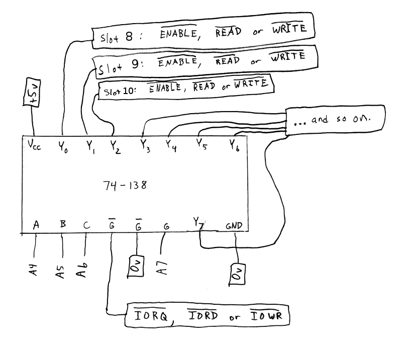
Two 3-to-8 decoders are actually cheaper than one 4-to-16 decoder, so I totally recommend this.
Needless to say, the rest of the bus board is just a bunch of bus lines:
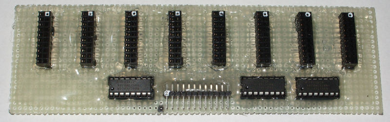
(Note: The pinout on this board is a bit different, due to being the very first board I built, before I had the design completely worked out. So don't look too closely. I've since rewrired the affected pins, but no longer have the board and so I can't take another photo, and my newer board isn't as photogenic.)
The power lines, D0 through D7, A0 through A3, and the RESET signal of all I/O card slots are connected directly to the CPU & memory board connector.
Connector Types
For all connectors I've chosen to use header pin connectors. Card edges are cheaper if you produce circuit boards, but card edge connectors aren't so cheap, and circuit boards aren't so cheap and aren't easy to produce.The card slots are female connectors for two reasons:
1. Right-angle header pins are easy to find. Also, it's quite easy to put straight header pins on the edge of a board. (I just tie mine to the boards with fishing line threaded between each row of pins, then cover in hot glue.) I don't think I've ever even seen a right-angle female header connector.
2. Female headers are more expensive. This makes sense if you assume that you'll make more I/O cards than you'll have slots on your bus board. In reality, I doubt this will ever actually happen, and so this is kind of an anti-reason.
I guess it's hardly solid reasoning, but it's my reasoning.
2. Female headers are more expensive. This makes sense if you assume that you'll make more I/O cards than you'll have slots on your bus board. In reality, I doubt this will ever actually happen, and so this is kind of an anti-reason.
The connector to the CPU & Memory board cable is male header pins, for the obvious reason that this allows connecting the two boards with a ribbon cable. If only I could afford ribbon cables. Maybe some day...
Power Board
An ideal solution for the power board remains elusive.
The issue is the power-on reset. A quick search of the internet will reveal that no one knows how to do this correctly. The usual best solution is to wire a capacitor to charge via a resistor, and feed that into a schmitt trigger inverter, and to also put a diode in reverse polarity across the resistor to ensure the capacitor discharges quickly when power is removed. This generally works just fine, but it isn't perfect.
Personally, I prefer to use a 74HC123 to time the reset pulse. It generally seems to generate a pulse on power-up, though it isn't a design feature. I think it just happens because the capacitor is discharged. This has the added advantage that a reset button can be used as an input to the 74HC123 where its edge-triggered inputs ensure that the reset pulse is of limited duration even if the reset button is held down, which is useful as some LCD displays don't do so well when the reset signal is held active for too long as the drivers remain active on the same row of pixels the whole time. However, this still fails to address the issue of brown-outs.
There are chips designed specifically to generate power-on reset signals, but they're expensive, and some are quite lame in that they too fail to address issues of brown-outs or excessively long voltage rise times, which is quite silly since being able to deal with such situations is about the only reason I'd ever consider spending $10 on an IC that does nothing besides generate a reset signal.
My plans for my next design are simply to use an ATtiny13A. It's a $1 microcontroller that features its own power-on reset and brown-out detection. So I'm going to program it to hold an output pin high for a moment, then lower it, then just loop waiting for a signal on another pin that it should generate another reset pulse. It's kind of a lame use of a microcontroller, but fuck, it seems to be the cheapest and most ideal solution to this problem.
Anyway, just add power in there somewhere, and activate your reset signal one way or another, and you're good to go.
So...
Send comments and questions to my email address.