SPI SD Card Interface for Z80 Systems
This web page documents a high-speed SPI interface I built for a Z80 system. It is capable of transferring a byte in just 1 µs.Assembly Interface
Bytes are transferred through the interface with this simple assembly code:
First the byte to be transmitted is written to port 0, then a write to port 1 causes the SPI transfer to take place. Finally, a read from port 0 retrieves the received byte. My notes indicate that no "nop" instructions are required before the "in" instruction, but I was probably using one of those old 4 MHz Z80 chips at the time. A 10 MHz chip probably requires two "nop" instructions and a 20 MHz chip probably requires six, unless you use a faster clock for the SD transfer. The limit on the SPI clock is probably going to be the counter chip you use in the circuit below. The SD cards themselves are already designed to transfer data at insane speeds.
Anyway, just for fun, here's an oscilloscope image of the eight clock cycles necessary to transfer a byte, initiated by the second "out" instruction, followed by the read pulse generated by the Z80 in response to the "in" instruction:
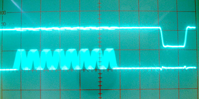
The inconsistent offset of the SPI clock is due to its clock being independant of the Z80 clock. If you want to test how many "nop" instructions you need, keep in mind that as long as those eight clocks are finished before the start of the pulse, it is close enough, as the Z80 doesn't sample the data on the bus until after 80% of the duration of the read pulse has completed.
transfer_byte:
  out $00
receive_byte:
  out $01
  in $00
ret
Anyway, just for fun, here's an oscilloscope image of the eight clock cycles necessary to transfer a byte, initiated by the second "out" instruction, followed by the read pulse generated by the Z80 in response to the "in" instruction:
The inconsistent offset of the SPI clock is due to its clock being independant of the Z80 clock. If you want to test how many "nop" instructions you need, keep in mind that as long as those eight clocks are finished before the start of the pulse, it is close enough, as the Z80 doesn't sample the data on the bus until after 80% of the duration of the read pulse has completed.
Schematics
This is how the SD card is connected.
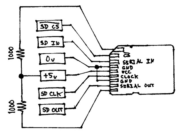
While SD cards technically aren't supposed to be powered by 5 volts, I've yet to see any bad consequences from doing so, and doing so avoids a lot of effort in converting voltage levels. You may want to look into using proper voltages though if you can't afford to fry your SD card. Techically you're supposed to use a voltage specified by the card in some data you can read from it (presumably while using some random voltage like 3.3 volts), but that structure doesn't even have bits to specify whether the card supports 5 volts, so I decided not to worry about it and just try it anyway. I've stuck a few different cards in it, so far it hasn't killed any of them yet.
The clock for the SPI transfer comes from a 16 MHz crystal that is then divided by 2 by a 4-bit counter, which also counts out exactly 8 pulses.
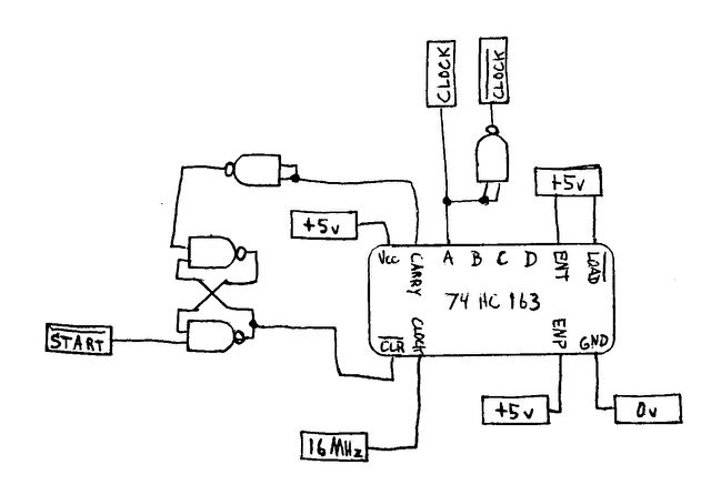
The reason for using the counter chip's "A" output as the SD clock is that, when the Z80 triggers a transfer, I don't want the transfer to begin with a fraction of a clock pulse, whatever remains of the current pulse when the Z80 initiates the transfer. As the counter is counting those partial clocks, it'll either count that initial fractional pulse, or it won't, but either way, it's "A" output is only going to be complete pulses of full duration. So that output is used to clock the SPI transfer instead of using the 16 MHz clock directly.
The clock circuit is controlled by this circuit:
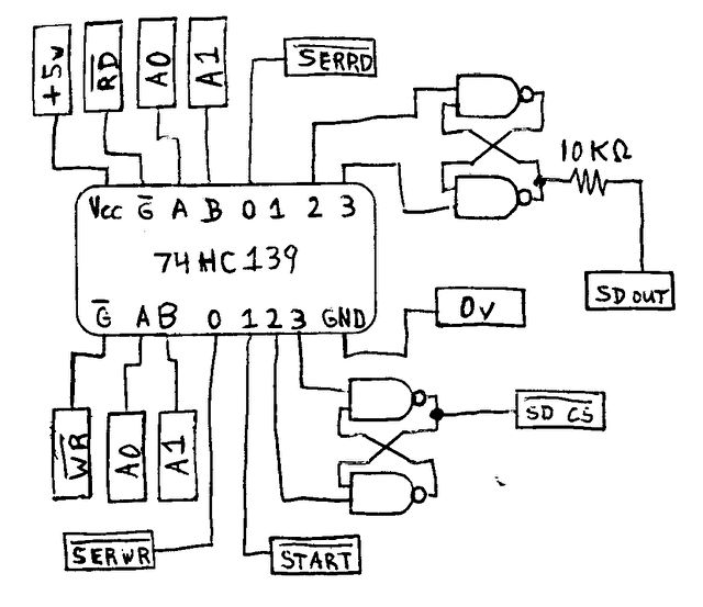
Note that my Z80 bus design is such that the "read" and "write" signals are only active when a particular card slot's I/O range is active, and so I don't have to decode anything besides A0 and A1. If your system works differently, then you will need to attach additional decoding circuitry where the /RD and /WR inputs attach.
Anyway, this sets up port 0 to read/write the shift registers. A write to port 1 then starts the SPI transfer. Ports 2 & 3 when written to toggle the /CS on the SD card, with port 2 lowering /CS and port 3 raising it. Ports 2 & 3 when read from similarly toggle a pull-up / pull-down resistor attached to the SD card's data output pin, which can be used to detect if a card is present by changing the polarity and noting whether the bits read from the interface continue to match the pull-up / pull-down, so that an empty card slot looks different than an unresposive but present card.
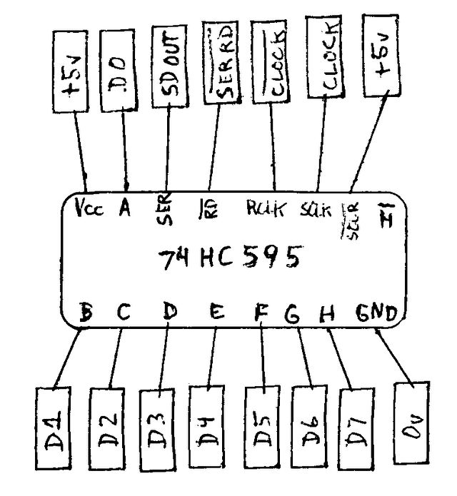
This is the circuit for the output shift register:
The serial data input pin is tied high so that if the Z80 doesn't write anything to the register before initiating a transfer, the register will simply output all of the high bits it shifted in when shifting out the previous byte.
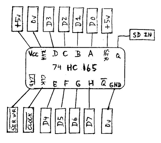
This is the circuit for the input shift register:
Note the polarity of the two clock inputs. It uses both the inverted and non-inverted clocks so that the register latch is activated well after the final bit is shifted into the register.
While SD cards technically aren't supposed to be powered by 5 volts, I've yet to see any bad consequences from doing so, and doing so avoids a lot of effort in converting voltage levels. You may want to look into using proper voltages though if you can't afford to fry your SD card. Techically you're supposed to use a voltage specified by the card in some data you can read from it (presumably while using some random voltage like 3.3 volts), but that structure doesn't even have bits to specify whether the card supports 5 volts, so I decided not to worry about it and just try it anyway. I've stuck a few different cards in it, so far it hasn't killed any of them yet.
The clock for the SPI transfer comes from a 16 MHz crystal that is then divided by 2 by a 4-bit counter, which also counts out exactly 8 pulses.
The reason for using the counter chip's "A" output as the SD clock is that, when the Z80 triggers a transfer, I don't want the transfer to begin with a fraction of a clock pulse, whatever remains of the current pulse when the Z80 initiates the transfer. As the counter is counting those partial clocks, it'll either count that initial fractional pulse, or it won't, but either way, it's "A" output is only going to be complete pulses of full duration. So that output is used to clock the SPI transfer instead of using the 16 MHz clock directly.
The clock circuit is controlled by this circuit:
Note that my Z80 bus design is such that the "read" and "write" signals are only active when a particular card slot's I/O range is active, and so I don't have to decode anything besides A0 and A1. If your system works differently, then you will need to attach additional decoding circuitry where the /RD and /WR inputs attach.
Anyway, this sets up port 0 to read/write the shift registers. A write to port 1 then starts the SPI transfer. Ports 2 & 3 when written to toggle the /CS on the SD card, with port 2 lowering /CS and port 3 raising it. Ports 2 & 3 when read from similarly toggle a pull-up / pull-down resistor attached to the SD card's data output pin, which can be used to detect if a card is present by changing the polarity and noting whether the bits read from the interface continue to match the pull-up / pull-down, so that an empty card slot looks different than an unresposive but present card.
This is the circuit for the output shift register:
The serial data input pin is tied high so that if the Z80 doesn't write anything to the register before initiating a transfer, the register will simply output all of the high bits it shifted in when shifting out the previous byte.
This is the circuit for the input shift register:
Note the polarity of the two clock inputs. It uses both the inverted and non-inverted clocks so that the register latch is activated well after the final bit is shifted into the register.