Z80 EEPROM Programmer
The following describes how to build a Z80 system with EEPROM which can be programmed over a USB link from a PC, without requiring a pre-programmed EEPROM. This design is ideal because of the following reasons:
1. It does not require a pre-programmed EEPROM, and so it is suitable for those who do not already have an EEPROM programmer.
2. It can program EEPROMs in about 5 seconds, which is way faster than the 5 minutes that some commercial EEPROM programmers require.
3. The same system can program EEPROMs and then run the code in those EEPROMs, so there is no need to swap chips around when developing code.
4. The PC can automatically switch the system in to and out of EEPROM programming mode, so you don't have to push any buttons or flip any switches.
I don't think it gets any easier than that.
2. It can program EEPROMs in about 5 seconds, which is way faster than the 5 minutes that some commercial EEPROM programmers require.
3. The same system can program EEPROMs and then run the code in those EEPROMs, so there is no need to swap chips around when developing code.
4. The PC can automatically switch the system in to and out of EEPROM programming mode, so you don't have to push any buttons or flip any switches.
An Example
Here's a picture just in case you're wondering how much work is involved:
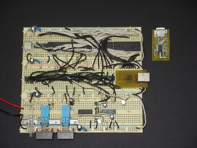
The largest hurdle to building this circuit is that it requires either an FT240X ($2.16) or an FT245R ($4.50), neither of which is available in DIP form. However, there are development boards available for each, $20.00 for the FT245R and $23.75 for the FT240X.
Persuaded by those high prices (which matter a lot more when you realize this chip is so useful that you want ten of them) I designed my own board for the FT245RL which I made at home and which is shown in the photos above. (Here is the board in Postscript in case you want to make one as well.) With the recent introduction of the lower-cost FT240X, I created a set of Gerber files to be manufactured by dirtypcbs.com for a mere $14 for ten. With these boards I was able to create my own FT240X boards for a mere $4.76 each, including the cost of all of the components.
Anyway, once you're past that hurdle, the rest isn't terribly difficult. A logic analyzer or an oscilloscope might be helpful for debugging, but it isn't required, as careful attention to and verification of the wiring is sufficient to make the circuit operate.
The Basic Idea
A USB link to a PC is provided by one of the above-mentioned FTDI chips, which provide a simple 8-bit parallel I/O port. To overcome the lack of a pre-programmed ROM, when in programming mode, the system accesses this I/O port in place of normal memory. The PC sends a sequence of bytes that the Z80 reads as a series of instructions to execute. These instructions program the system's SRAM with a small program which is used to program the EEPROM. The EEPROM isn't programmed directly because the high-speed multi-byte programming capability of the AT28C256 ($7.50) requires that bytes be written over a very short period of time, and delays from the USB link may prevent that, so the data to be written to the EEPROM and the code which writes it are written to SRAM to ensure that the operation runs smoothly. Once the EEPROM is programmed and verified, the system is reset with a new memory map that causes the Z80 to boot the EEPROM. This all happens in about four seconds.
Beginner Stuff
The following schematics detail only the specifics of this programming interface, and assume that you otherwise know how to build a Z80 system. If you don't already know how to build a Z80 system, then you probably have issues far beyond this page lacking full schematics, but this page which also lacks full schematics may be of some help. On the other hand, if you're just looking for a bit of reassurance that you're understanding everything, here's a quick list of everything that isn't included in the schematics below:
- Power must be supplied to all chips.
- All data lines of all chips must be connected to all corresponding data lines of all other chips.
- All address lines of all chips must be connected to all corresponding address lines of all other chips, the exception being A15 which is described below, as it is used to select between RAM and EEPROM.
- You'll want a reset circuit of some kind, capable of providing a reset signal at power on, though the reset circuit shown below should work even without one.
- You'll need to give the Z80 an appropriate clock signal.
- The Z80 inputs BUSREQ, INT, and NMI should be tied high unless you have other plans for them. If you do have other plans, you'll want to OR the inputs you would attach to those pins with the BURN signal described below, so that those pins remain high during the programming procedure.
- The FTDI chip will need to be connected to a USB connector, as described in its datasheet.
Notes about My Schematic Style
I'll present the design as a series of tiny schematics, since I think that understanding it is easier that way. A single large schematic may show the entire circuit at once, but it takes a long time to trace all of those lines and understand how the circuit operates. By using many small schematics, it's easy to explain what happens at each step, what each signal represents, and how it is all supposed to work together.
Note that the chip designations like "74-123" should be whatever flavor of the 74 series you prefer, e.g. I use a "74HC123" as I prefer the CMOS level inputs, but many prefer the "74HCT123" with TTL-compatible inputs, and for whatever reason, some still use the "74LS123" which consumes more power and has excessive input current requirements. Just make sure that whatever you choose is compatible with the Z80, EEPROM and SRAM you are using. Modern low-power chips are CMOS, but the older TTL varieties still exist, so you may have either one, in which case the HCT series is a safe choice since the inputs and outputs are compatible with both CMOS and TTL.
Note that the chip designations like "74-123" should be whatever flavor of the 74 series you prefer, e.g. I use a "74HC123" as I prefer the CMOS level inputs, but many prefer the "74HCT123" with TTL-compatible inputs, and for whatever reason, some still use the "74LS123" which consumes more power and has excessive input current requirements. Just make sure that whatever you choose is compatible with the Z80, EEPROM and SRAM you are using. Modern low-power chips are CMOS, but the older TTL varieties still exist, so you may have either one, in which case the HCT series is a safe choice since the inputs and outputs are compatible with both CMOS and TTL.
The Schematics
First, the system needs to have two states, one which behaves as a normal Z80 system, the other which allows programming of the EEPROM from the PC.
To switch between these two states, the following circuit is used:
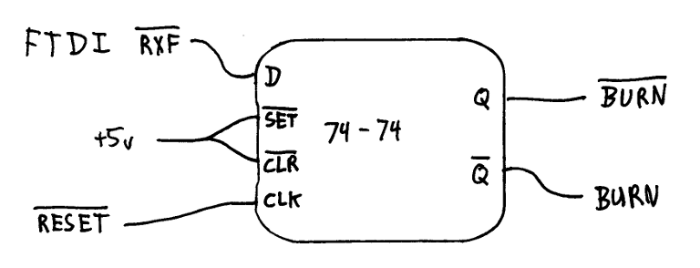
The PC will only send data when programming the EEPROM is desired, and so this circuit causes the state of the USB chip's -RXF signal, which indicates that data is in the USB chip's buffer and may be read, to be latched as a -BURN signal after each system reset.
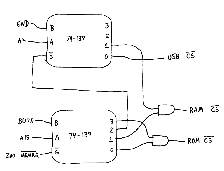
Next, the system needs to have two different memory maps according to whether it is in EEPROM programming mode:
Thus, our programming mode will boot by reading instructions from the USB chip, and has 16 kB of SRAM at its disposal so that it may cache data, which enables the use of the high-speed programming mode of the AT28C256.
To achieve these two memory maps, a single 74-139 (which contains two 2 to 4 decoders) and two AND gates are used:
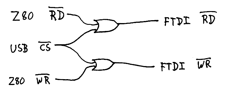
The USB chip doesn't have a chip select, and so the following circuit is used:
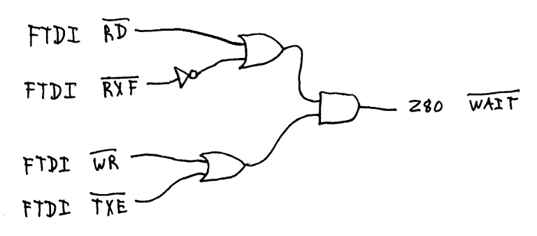
Also, the Z80 needs to wait until data is available in the USB chip's buffer before reading data, and until the USB chip's FIFO has space available before writing data. This circuit activates the Z80's -WAIT signal to ensure it waits when necessary.
Finally, it would be nice if the -RESET signal were activated automatically when a switch to or from programming mode was desired. You can leave this part out and just press the reset button manually after starting the programming procedure and after it finishes, but it's easy to automate as well, using the following algorithm:
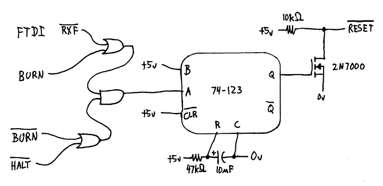
As a power-on reset circuit, it naturally sucks, as the requirements for such a circuit (it always works, even for very brief power-off conditions, and it detects brown-outs as well) are apparently an impossible goal, as no one seems to be able to design a good solution. So you may want to design your own reset circuit if you don't like mine. In any event, this circuit causes the signal on the A input of the 74-123 to go low when a reset is required, which triggers a pulse from the 74-123, which activates the -RESET signal, causing the 74-74 in the first schematic to latch the new state, and it will likely generate a power-on reset signal for you as well.
To switch between these two states, the following circuit is used:
The PC will only send data when programming the EEPROM is desired, and so this circuit causes the state of the USB chip's -RXF signal, which indicates that data is in the USB chip's buffer and may be read, to be latched as a -BURN signal after each system reset.
Next, the system needs to have two different memory maps according to whether it is in EEPROM programming mode:
| Address Range | Normal Mode | Programming Mode |
|---|---|---|
| $0000 - $3FFF | EEPROM | USB |
| $4000 - $7FFF | SRAM | |
| $8000 - $BFFF | SRAM | EEPROM |
| $C000 - $FFFF |
Thus, our programming mode will boot by reading instructions from the USB chip, and has 16 kB of SRAM at its disposal so that it may cache data, which enables the use of the high-speed programming mode of the AT28C256.
To achieve these two memory maps, a single 74-139 (which contains two 2 to 4 decoders) and two AND gates are used:
The USB chip doesn't have a chip select, and so the following circuit is used:
Also, the Z80 needs to wait until data is available in the USB chip's buffer before reading data, and until the USB chip's FIFO has space available before writing data. This circuit activates the Z80's -WAIT signal to ensure it waits when necessary.
Finally, it would be nice if the -RESET signal were activated automatically when a switch to or from programming mode was desired. You can leave this part out and just press the reset button manually after starting the programming procedure and after it finishes, but it's easy to automate as well, using the following algorithm:
1. When not in programming mode, and when data is available to read from the USB chip, reset the Z80 system, as this indicates that the PC wishes to program the Z80. (The PC will never send data to the USB chip otherwise, as its only purpose is programming the Z80.)
2. When in programming mode, we can't rely on the USB chip's buffer being empty as indicating anything, as PCs are good at pausing for no reason in particular. Instead, we can utilize the Z80's -HALT signal. Normally it will remain high, but at the end of the programming procedure, the PC can simply send a HLT instruction to the Z80, which will lower the Z80's -HALT signal, indicating that programming is complete. So, when in programming mode, and the -HALT signal is low, we reset the Z80 system again.
Here's one circuit that can accomplish this:
2. When in programming mode, we can't rely on the USB chip's buffer being empty as indicating anything, as PCs are good at pausing for no reason in particular. Instead, we can utilize the Z80's -HALT signal. Normally it will remain high, but at the end of the programming procedure, the PC can simply send a HLT instruction to the Z80, which will lower the Z80's -HALT signal, indicating that programming is complete. So, when in programming mode, and the -HALT signal is low, we reset the Z80 system again.
As a power-on reset circuit, it naturally sucks, as the requirements for such a circuit (it always works, even for very brief power-off conditions, and it detects brown-outs as well) are apparently an impossible goal, as no one seems to be able to design a good solution. So you may want to design your own reset circuit if you don't like mine. In any event, this circuit causes the signal on the A input of the 74-123 to go low when a reset is required, which triggers a pulse from the 74-123, which activates the -RESET signal, causing the 74-74 in the first schematic to latch the new state, and it will likely generate a power-on reset signal for you as well.
The Software
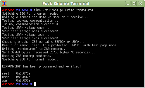
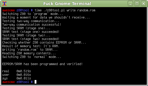
I've written a Perl script which runs in Linux which can program RAM in 0.5 seconds, AT28C256 EEPROMs in 3.9 seconds, and some other EEPROMs without page write mode in anywhere from 0 to 5 minutes depending on how many bytes need to be changed. It can also activate and deactivate the software write protection of AT28C256 chips, as well as simply read the data already programed into an EEPROM and save it to a file.
The script doesn't work in Windows, and I don't know how to make it work, but I suspect it isn't too difficult for someone who knows how. I tried making it open "COM1" instead of the Linux device file for the FTDI chip, but it seems select() doesn't work on COM1. Then I was going to try the Win32::Serial module, but the CPAN tool for Strawberry Perl was hopelessly broken, and so I couldn't install the module. So I gave up. However, if you figure out how to make it work in Windows, I'm sure others would appreciate your work, so please send me your changes and I'll host them here.
In case you prefer to write your own code, here is the general procedure:
1. If you're using Linux, you can't simply open the relevant /dev/ttyUSBx file and use it. Linux assumes that any serial port is a TTY and does weird shit as a result, namely, any bytes that come in the port are automatically sent back out, no data is readable at all until a character 13 received, and when it is, it's turned into a character 10 before being given to the program. You have to tell Linux not to do all of this BS. Granted, these USB chips have nothing in common with a serial port: They have no baud rate, no variable number of I/O bits, no stop bits, etc., and so it should simply be a character device, but for some fucking reason it isn't. Indeed, why all of this BS is the default setting of serial ports anyway is a good question, as even actual serial ports most often require the data to be unmolested during transfer. ...but, fuck, what do you expect from Linux? Anyway, a good "stty -F /dev/ttyUSB0 raw -echo" fixes things up, at least when the command will execute. Often the part of the kernel that handles serial ports locks up, and this command will never complete, in which case you need to disconnect the USB device and reconnect it. I've found that flaky USB hubs can make this problem worse, but it seems to occasionally happen no matter what, so be prepared to detect the condition and advise the user about how to resolve it. There's also a way to do what the 'stty' command does via ioctl() in C, but good luck finding documentation on that. ...and also, don't ever write more than 4096 bytes in a single system call to the port, or attempt to read more than 4096 bytes in a single system call, as you'll encounter all sorts of problems if you do.
In Windows, I have no clue what is necessary to open the serial port provided by the FTDI driver, but I'm sure it's nowhere near as much of a pain in the ass.
2. Send a short series of no-op instructions (zero bytes) to the Z80. Not too many, just enough that if the Z80 is half-way through reading a multi-byte opcode, it'll complete that opcode and be ready to read the beginning of another. Normally this won't be necessary, as the Z80 has just been reset and the USB chip's buffer should have been empty before you sent anything to it, but again, it's best to prevent weird conditions from screwing everything up, and who knows what has been sent to the serial port (especially in Linux, with its automatic echoing of bytes received on the port) before this programming procedure was started.
3. Send the byte sequence C3 00 00, which is the Z80 instruction "JMP $0000" which will reset the program counter to zero. You should do this occasionally throughout this entire process, as the USB chip is only read from when the Z80 reads from the memory range $0000 through $3FFF, and so if the program counter gets outside of this range, it will start looking to SRAM for instructions instead, and thus you'll lose control of the Z80. Remember, the Z80 has no cache, so you can jump as often as you like and it won't set up any sort of loop as the Z80 will always look to the USB chip for the next instruction byte, as it has always forgotten what it read from that address last time.
4. Continuously read data from the USB chip until you stop receiving it. A time-out of about a second is fine. Normally there shouldn't be any, but if for some reason there is (again, Linux's BS), the following steps won't complete correctly, so you need to get it out of the way. If the data never stops coming, then the Z80 must be executing EEPROM or SRAM addresses. This can happen if you interrupt the programming process midway, when it is executing SRAM code. In this case manually resetting the Z80 system will resolve the issue.
5. Test that two-way communication with the Z80 is functional. This might not be the case if you opened the wrong serial port, or the Z80 system is turned off, or the Z80 system is simply built incorrectly. You can do this by sending byte sequences like this:
21 00 00 - The "ld hl $0000" instruction, so that HL points to the USB chip's address space. This only needs to be done once.
7E - The "ld a [hl]" instruction, which then causes the Z80 to read a single byte from the USB chip and store it in the A register.
xx - Any random test byte, which is read by the previous instruction as the data at address $0000.
77 - The "ld [hl] a" instruction, which causes the Z80 to write that random byte in the A register back to the USB chip.
Note that, while it may seem logical to use the LDIR instruction to transfer many such bytes, the LDIR instruction is implemented in the Z80 by simply failing to increment the PC register. Thus, as it loops, it repeatedly re-reads the instruction, and so you would repeatedly have to re-send the instruction. Thus, there isn't any point to it, as it is a two-byte instruction and so you end up sending exactly the same amount of data to make this happen.
Anyway, just use this process to send a dozen random bytes, then verify that you read those same bytes back from the USB chip. Obviously, if this step fails, you may not read any data, and so you must be prepared to detect this condition as well.
6. Send a series of Z80 instructions (similar to how step 5 works) to cause an EEPROM burning program (like this one, in Sarcasm syntax) to be written to the SRAM. This code needs to simply read a 64 byte block of data from the PC and store it to SRAM, then copy the 64 bytes from SRAM to the correct EEPROM address, then wait until the EEPROM indicates that the programming of that block is complete, then repeat until the entire EEPROM is programmed, then return control back to the PC by executing a "JMP $0000" instruction.
7. Send a JMP instruction to the Z80 so that it executes the EEPROM burning program you just loaded into SRAM.
8. Send the EEPROM data, which will be received by the EEPROM burning program, temporarily stored (in 64 byte chunks) in SRAM, then written to the EEPROM.
9. If desired (and I think it is), write another program to SRAM that reads the EEPROM data and sends it back to the PC, in order to verify that the EEPROM was written correctly. Note that this adds only milliseconds to the programming procedure, whereas an incorrectly-programmed EEPROM can add hours to the debugging process.
10. Assuming the EEPROM is correctly programmed, and so it is time to execute the code it contains, send a single HLT instruction to the Z80, to trigger the automatic reset circuit shown above.
...but of course, it would be a lot easier to simply use my software instead.
In Windows, I have no clue what is necessary to open the serial port provided by the FTDI driver, but I'm sure it's nowhere near as much of a pain in the ass.
2. Send a short series of no-op instructions (zero bytes) to the Z80. Not too many, just enough that if the Z80 is half-way through reading a multi-byte opcode, it'll complete that opcode and be ready to read the beginning of another. Normally this won't be necessary, as the Z80 has just been reset and the USB chip's buffer should have been empty before you sent anything to it, but again, it's best to prevent weird conditions from screwing everything up, and who knows what has been sent to the serial port (especially in Linux, with its automatic echoing of bytes received on the port) before this programming procedure was started.
3. Send the byte sequence C3 00 00, which is the Z80 instruction "JMP $0000" which will reset the program counter to zero. You should do this occasionally throughout this entire process, as the USB chip is only read from when the Z80 reads from the memory range $0000 through $3FFF, and so if the program counter gets outside of this range, it will start looking to SRAM for instructions instead, and thus you'll lose control of the Z80. Remember, the Z80 has no cache, so you can jump as often as you like and it won't set up any sort of loop as the Z80 will always look to the USB chip for the next instruction byte, as it has always forgotten what it read from that address last time.
4. Continuously read data from the USB chip until you stop receiving it. A time-out of about a second is fine. Normally there shouldn't be any, but if for some reason there is (again, Linux's BS), the following steps won't complete correctly, so you need to get it out of the way. If the data never stops coming, then the Z80 must be executing EEPROM or SRAM addresses. This can happen if you interrupt the programming process midway, when it is executing SRAM code. In this case manually resetting the Z80 system will resolve the issue.
5. Test that two-way communication with the Z80 is functional. This might not be the case if you opened the wrong serial port, or the Z80 system is turned off, or the Z80 system is simply built incorrectly. You can do this by sending byte sequences like this:
21 00 00 - The "ld hl $0000" instruction, so that HL points to the USB chip's address space. This only needs to be done once.
7E - The "ld a [hl]" instruction, which then causes the Z80 to read a single byte from the USB chip and store it in the A register.
xx - Any random test byte, which is read by the previous instruction as the data at address $0000.
77 - The "ld [hl] a" instruction, which causes the Z80 to write that random byte in the A register back to the USB chip.
Note that, while it may seem logical to use the LDIR instruction to transfer many such bytes, the LDIR instruction is implemented in the Z80 by simply failing to increment the PC register. Thus, as it loops, it repeatedly re-reads the instruction, and so you would repeatedly have to re-send the instruction. Thus, there isn't any point to it, as it is a two-byte instruction and so you end up sending exactly the same amount of data to make this happen.
Anyway, just use this process to send a dozen random bytes, then verify that you read those same bytes back from the USB chip. Obviously, if this step fails, you may not read any data, and so you must be prepared to detect this condition as well.
6. Send a series of Z80 instructions (similar to how step 5 works) to cause an EEPROM burning program (like this one, in Sarcasm syntax) to be written to the SRAM. This code needs to simply read a 64 byte block of data from the PC and store it to SRAM, then copy the 64 bytes from SRAM to the correct EEPROM address, then wait until the EEPROM indicates that the programming of that block is complete, then repeat until the entire EEPROM is programmed, then return control back to the PC by executing a "JMP $0000" instruction.
7. Send a JMP instruction to the Z80 so that it executes the EEPROM burning program you just loaded into SRAM.
8. Send the EEPROM data, which will be received by the EEPROM burning program, temporarily stored (in 64 byte chunks) in SRAM, then written to the EEPROM.
9. If desired (and I think it is), write another program to SRAM that reads the EEPROM data and sends it back to the PC, in order to verify that the EEPROM was written correctly. Note that this adds only milliseconds to the programming procedure, whereas an incorrectly-programmed EEPROM can add hours to the debugging process.
10. Assuming the EEPROM is correctly programmed, and so it is time to execute the code it contains, send a single HLT instruction to the Z80, to trigger the automatic reset circuit shown above.
Contact Information
Send comments and questions to my email address.